'India's first wafer from Dholera semiconductor plant likely in 2028': Ashwini Vaishnaw
Ashwini Vaishnaw said he has kept a single nail on a wall in his office empty, waiting for the first wafer to emerge from the Dholera plant. | India News
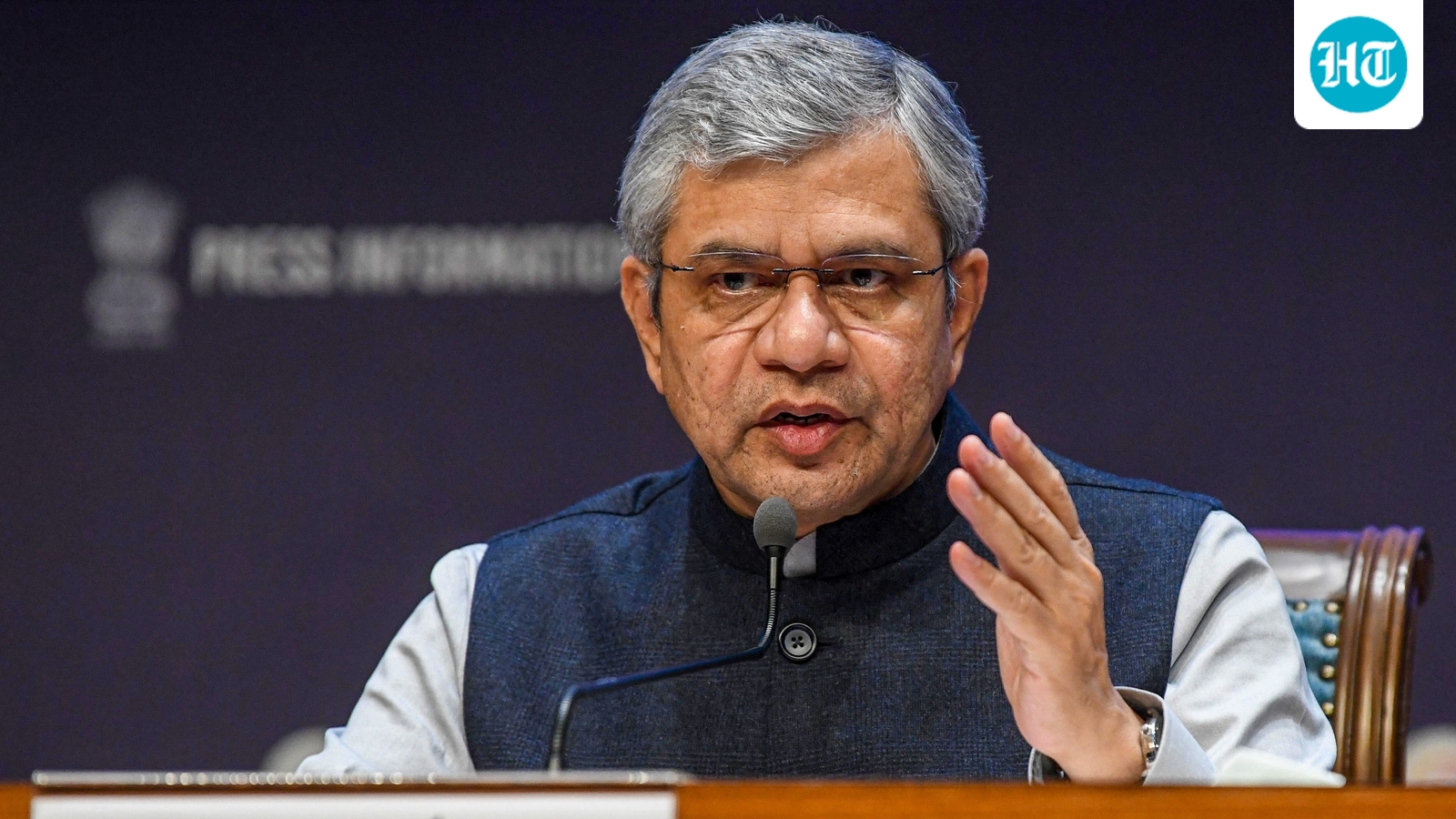
Ashwini Vaishnaw said he has kept a single nail on a wall in his office empty, waiting for the first wafer to emerge from the Dholera plant.
Electronics and IT minister Ashwini Vaishnaw said on Friday that he is waiting for the first wafer to come out of India’s first semiconductor fabrication plant in Dholera in 2028, as he said the country’s semiconductor industry had moved from establishing capacity to scaling up production.
During a fireside chat on the second day of Semicon India 2026 in New Delhi, Vaishnaw said he has kept a single nail on a wall in his office empty, waiting for the first wafer to emerge from the Dholera plant.
Also Read | Semicon 2.0 gets it right on the issues that matter
India Semiconductor Mission
Five semiconductor ATMP/OSAT (assembly, testing, making and packaging/outsource semiconductor assembly and test) plants out of the 12 selected in the first phase of the government’s India Semiconductor Mission have begun commercial production in India and are exporting their output as well as supplying Indian companies. The facilities are packaging and testing chips rather than fabricating them, with the minister saying they are able to compete on both cost and quality.
“Kaynes, CG Semi, CDIL, Suchi and Micron - all of them are rapidly expanding because whatever they produce, there is a market. So, demand is huge,” he said. “It’s now a question of being able to ramp up the production, and that is what the industry is currently focussed on.”
Also Read | Semiconductor plants, energy security: PM Modi renews push for ‘aatmanirbhar Bharat’
Tata Electronics fab in Gujarat
The Tata Electronics fab in Dholera, Gujarat, is scheduled to be commissioned in 2028, and Vaishnaw said a large part of its capacity was already booked.
The minister said the government’s semiconductor programme had been designed around a 20-year roadmap due to the complexity of the industry and the time required to build an ecosystem around fabs. Semicon 2.0, the second phase of the government’s semiconductor programme, is built around six pillars - chip design, materials and machines, more fabs, more ATMP units, research and development, and talent.
Also Read | PM says India-made chips have started reaching world: Where Semiconductor Mission stands
Vaishnaw said the government expects at least 200 chip-design companies to develop in India through Semicon 2.0. Under the first phase, more than 105 chip-design startups emerged and 20 received venture capital funding, he said.
I am a technology policy reporter with the National Political Bureau at Hindustan Times, based in New Delhi. I cover digital policy and the intersection of technology and society, focusing mainly on what's happening in India. My beat often involves tracking platform regulation, privacy, internet curbs, and the real-world impact of digital rules, among other things. Can usually be found reading government notifications so that you don't have to. I cover three key ministries: Ministry of Electronics and Information Technology (MeitY), Ministry of Communications, and the Ministry of Information and Broadcasting (I&B). I am originally from New Delhi and a graduate of the Asian College of Journalism, Chennai. Over the past nine years, I have worked across television, digital and print media with The Secretariat, CNN-News18, Tiranga TV, Interesting Engineering, and now Hindustan Times. Although I am not on X, I can be reached at sejal.sharma@hindustantimes.com for tips, a chat or book recommendations. I respond fast, usually within a couple of hours. Outside of work, I enjoy playing badminton and driving my car. I am a firm believer that every trip — work or leisure — deserves a fridge magnet.Read More